Welcome to Sankalp Semiconductor – your gateway to advanced and integrated semiconductor solutions. At Sankalp, we engineer success by encompassing the full spectrum of semiconductor services. Our holistic services spans from the intricate design of chip architecture to the sophisticated development of system software, ensuring a seamless transition from concept to reality.
Silicon NXT- Silicon Design & Platform Services
We empower you with a comprehensive suite of solutions to breathe life into your chip designs. From conception to realization, we bridge the gap between your vision and a fully functional silicon device.
Digital Design
We deliver RTL development, logic design, DFT and verification services, ensuring the flawless execution of your architecture.
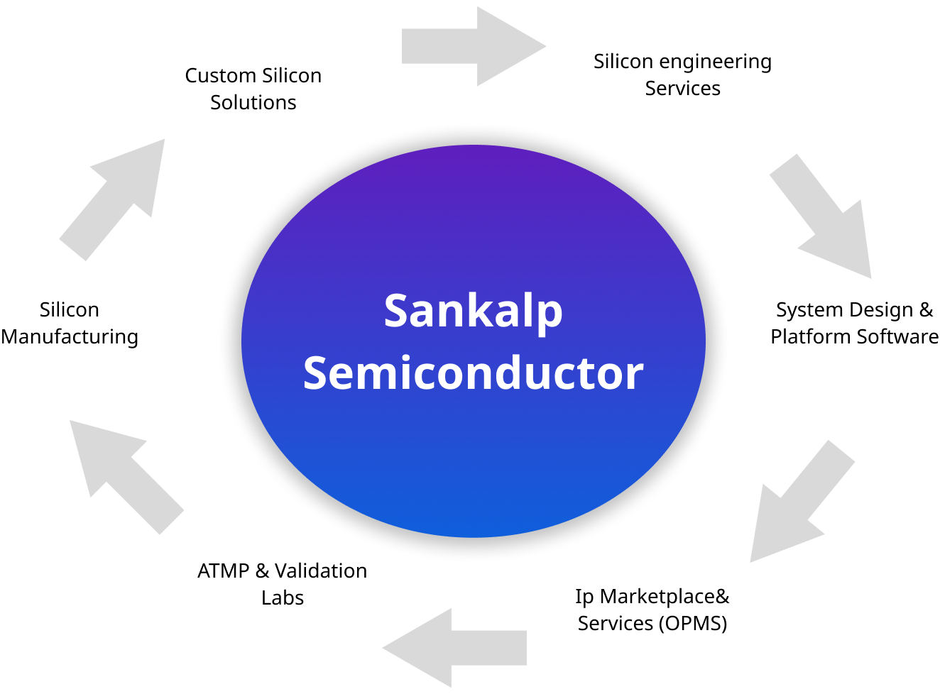
Sankalp Semiconductor provides custom silicon services. We help you build a chip that meets your specific needs ensuring optimal power, performance and area. We provide end-to-end services starting from specification definition to micro-architecture till high volume manufacturing, validation and qualification. We manage the complete supply chain, ensuring that products are delivered on time and to the highest quality standards. Click to know more.
Industries We Serve
Healthcare
Revolutionizing the healthcare industry with its semiconductor services, focusing on advanced solutions that cater to a wide range of medical applications.
Sankalp Semiconductor is redefining the automotive industry with specialized semiconductor services that cater to the rapidly evolving demands of the sector.
Helm of enabling sophisticated communication and connectivity solutions across the globe, our chip design services integrate state-of-the-art technologies.
Our expertise in chip design and development plays a critical role in transforming urban environments into smarter, more efficient, and sustainable spaces.
Lorem ipsum dolor sit amet consectetur. Mauris felis nunc sit gravida. Sit enim ornare condimentum non pulvinar nibh. Orci ac etiam vulputate.
7000+ Engineers
Lorem ipsum dolor sit amet consectetur. Mauris felis nunc sit gravida. Sit enim ornare condimentum non pulvinar nibh. Orci ac etiam vulputate.
Established Ecosystem Partners
Lorem ipsum dolor sit amet consectetur. Mauris felis nunc sit gravida. Sit enim ornare condimentum non pulvinar nibh. Orci ac etiam vulputate.
In-House Labs, Acelerators and Platforms
Lorem ipsum dolor sit amet consectetur. Mauris felis nunc sit gravida. Sit enim ornare condimentum non pulvinar nibh. Orci ac etiam vulputate.
Foundry Partners
IP Partners
Success Stories
Key benefits:
Early automated defect identification by comparing: images with a golden data image and detect/classify anomaly.
Improve the product quality.
Reduce manual effort more than 60%.
Client profile: A leading semiconductor equipment client sought assistance for inspecting equipment using Image processing technology to detect anomaly.
Key benefits:
The predictive model was deployed on tools at customer site and validated with real time data.
Predicted parameters needed no manual tuning as they generated good recipes.
Wafer implant interruptions due beam tuning parameter error reduced by 90% (implies yield improvement).
Client profile: The world’s leading ion implanter equipment manufacturer needed to predict the beam parameters and optimize tuning of the beam.