Sankalp Semiconductor

Services

ATMP Services

Lab Infra

OSAT Partnerships

Play Video

ATMP services

Sankalp Semiconductor offers Advanced Test and Measurement Program (ATMP) services, which involve the testing and measurement of semiconductor chips to ensure their functionality and performance meet specific requirements. These services are crucial in the semiconductor industry to guarantee the quality and reliability of integrated circuits before they are deployed in ATMP services
Our ATMP services, encompass a range of activities aimed at ensuring the quality, functionality, and reliability of semiconductor chips. ATMP services play a crucial role in the semiconductor industry by helping manufacturers produce high-quality, reliable chips that meet the stringent requirements of various applications, from consumer electronics to automotive and industrial devices.

Services

Test Development:

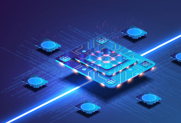
Designing and developing test programs and methodologies to assess the performance and functionality of semiconductor chips.

Wafer Testing:

Conducting tests on semiconductor wafers to identify defects and ensure the quality of individual chips before they are packaged.

Package Testing:

Testing individual semiconductor chips after they have been packaged to verify functionality and reliability.

Burn-in Testing:

Subjecting semiconductor chips to extended periods of stress testing to identify potential defects and ensure reliability over time.

Reliability Testing:

Evaluating the long-term performance and reliability of semiconductor chips under various operating conditions and environmental stresses.

LAB INFRA- Our Facility is spread over 40,000 SQ.FT, with 25,000 sq ft of clean room area (Class 10K and Class 1K) that can host 25+ testers & failure analysis test equipment and another 15,000 sq ft of Thermal Reliability test Lab and Silicon Warehousing facility. In the first Phase, the facility would offer front line test Platforms, Qual and FA equipment like:

 Testers:

Advantest V93K tester, Teradyne' ETS 364 and J750 testers with Tri-temp 12" wafer probers and Tri-Temp package handlers.

Qual Infra:

HTOL Thermal Chambers, HAST Chambers, Autoclave Chambers , Wire bond pull/ Shear Tester, ESD/Latch-up Tester,

 Failure Analysis Infra::

Microprober, 3D X ray, C-SAM, Scanning Electron Microscope, Digital Microscope with 6000x Zoom, I-V Curve Tracer.. etc..

The facility would complement our team of experts from Silicon NPI Engineering, Manufacturing Test Engineering along with the other Silicon Operations team to bring in rich experience to ensure seamless transition of programs to global FABs, OSATs, to ensure Silicon is not just designed but delivered to end users as part of our SPEC 2 PARTS delivery of Silicon parts.